We are pleased to announce a new publication in IPPT Reports on Fundamental Technological Research (IPPT Reports 3/2018): “A note on optical materials for photolithography applications”, by Amrita Jain, Agata Roszkiewicz and Wojciech Nasalski.
The objective of this report is to give a short review on different types of optical materials that can be used for various photolithography applications.
 |
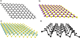
In the first section of the report, role of photoresist materials in lithography applications have been discussed. Photoresist materials are considered as one of the most important materials which are essentially required for the final fabrication of, mainly electronic, devices. So, this section is dedicated to the current state of art of photoresists development and their main parameters on which they depend. The second section describes the novel, currently emerging two-dimensional materials like graphene, hexagonal boron nitride (hBN) and transitional metal dichalcogenides (TMDs) which are nowadays considered as potential candidates as substrates for their use in the range of photolithographic processes. Figure 1 shows the lattice structures of various two dimensional materials. These materials are unique in their own way and have specific physical properties that play an important role in building high performance devices. |

Figure 1. Lattice structure of various two-dimensional materials: (a) monolayer graphene, (b) monolayer hexagonal boron nitride, (c) MoS2 monolayer (TMDC), (d) single layer black phosphorous
The third section is dedicated to the physical phenomena like diffraction, absorption and reflection which take place during photolithographic processes. Diffraction of light is an important parameter as it sets the limit of the maximum resolution therefore the minimum size of the individual elements which can be achieved. Further, photoresist also absorbs some portion of the exposing radiation in order to undergo a photochemical reaction. The optical effects that occur in the photoresist and substrate during exposure are important factors that influence the verticality of the photoresist walls. In this section these conditions are addressed in detail.
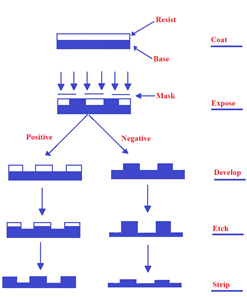
The last section is devoted to etching process; it is a process of material removing from the surface of other materials. There exist two types of etching; wet etching and dry etching. This process is considered as one of the most sophisticated processes for obtaining final patterns of photonic structures. Figure 2 shows the schematic representation of basic steps in photolithographic processes. It can be seen from the figure that several steps are involved for the pattering of structure like coating, exposing, developing etc. Out of all steps, etching is one of the most challenging steps in the entire process.

Figure 2. Schematic representation of basic steps in photolithographic processes
Moreover, in this section, the wet chemical etching of quartz substrate is discussed in detail, especially focusing on the structure of quartz and its influence on etching, mechanism of wet chemical etching and associated experimental aspects.
More: IPPT Reports


